Pcb Panel Design Rules

Pcb Panelization Methods Guidelines
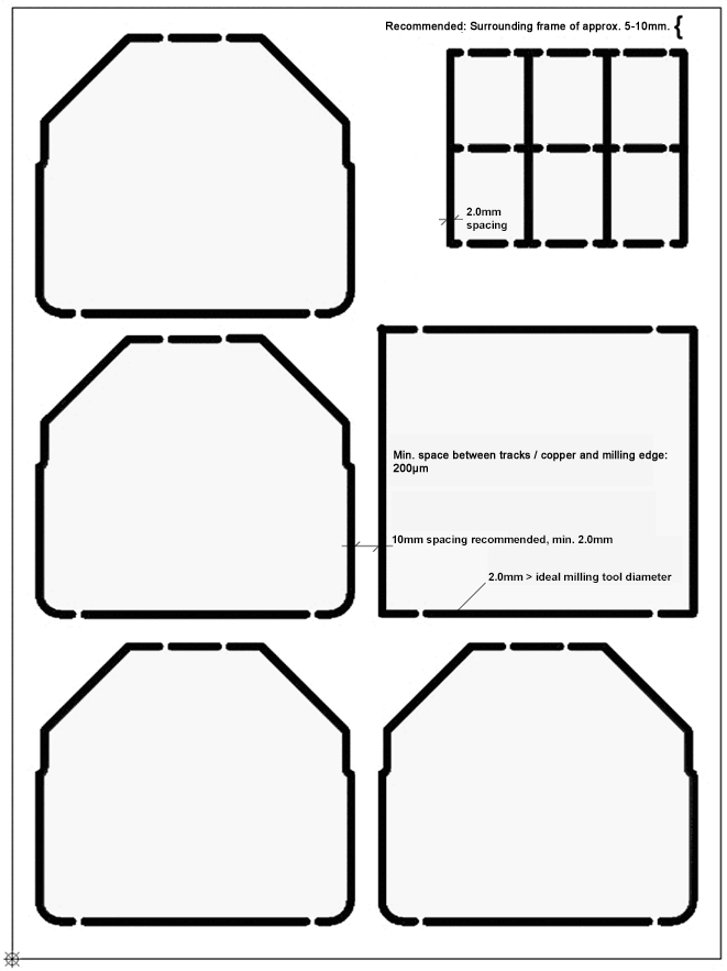
Realistic Design Rules For A Homemade Pcb Layout Kicad Info Forums
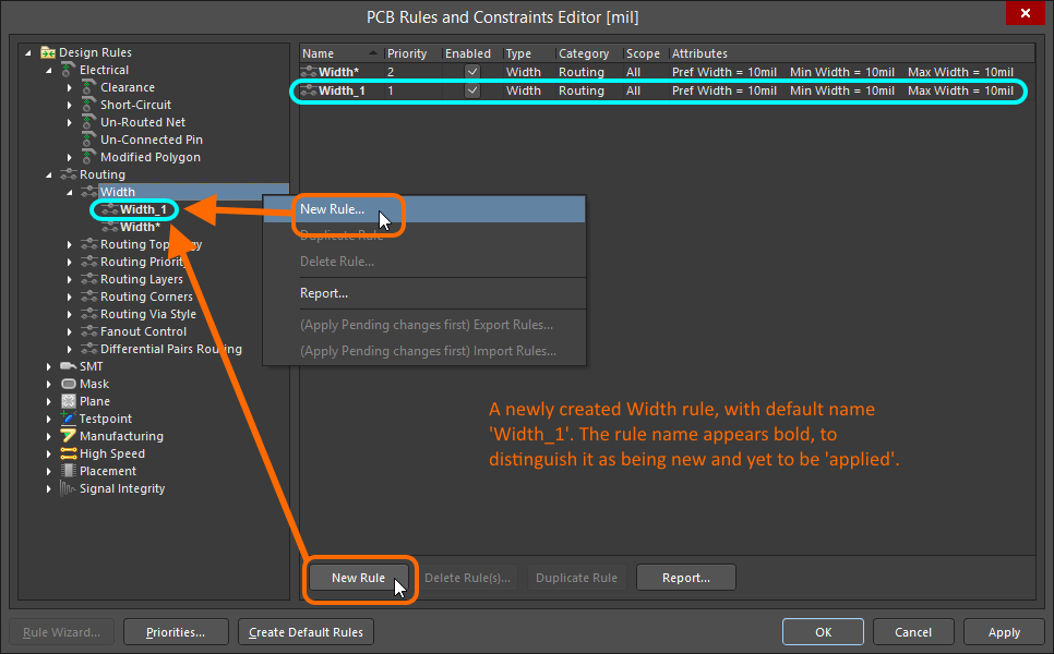
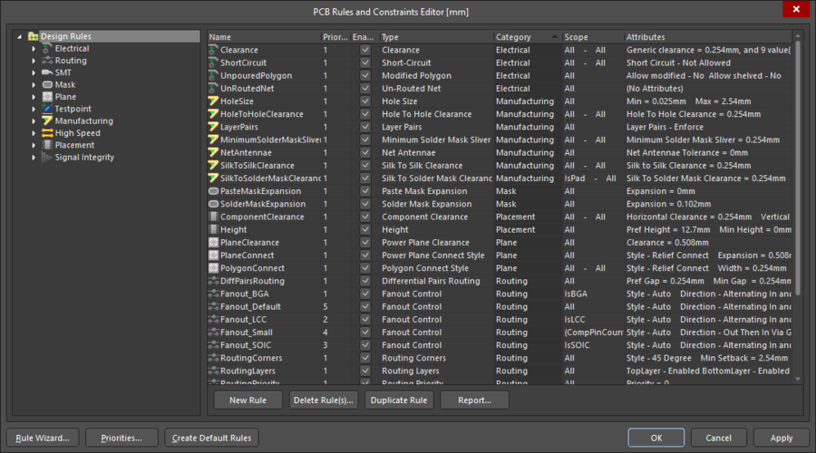
Constraining The Design Design Rules Altium Designer 19 1 User Manual Documentation

The Best 10 Practices Of Pcb Design Blog Jaapson Blog And Resource Center
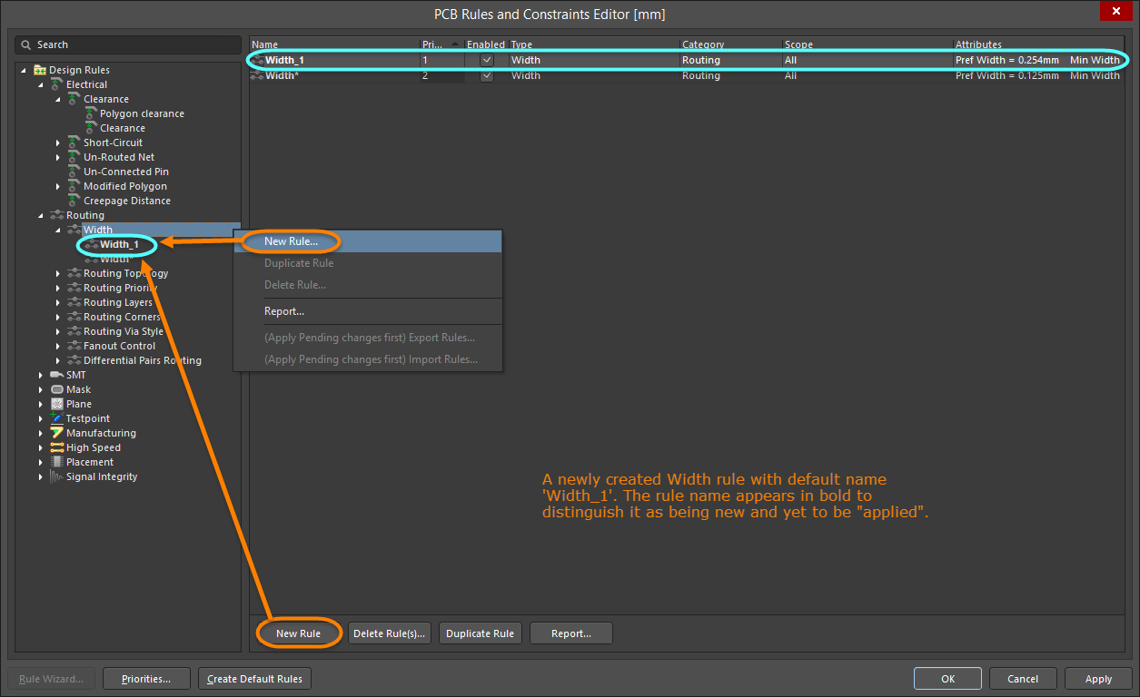
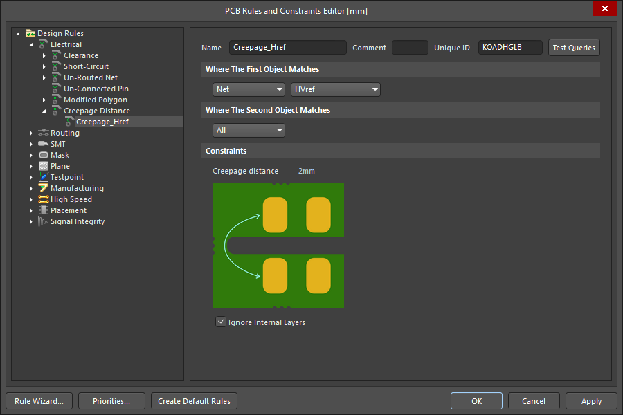
Constraining The Design Design Rules Altium Designer 20 2 User Manual Documentation
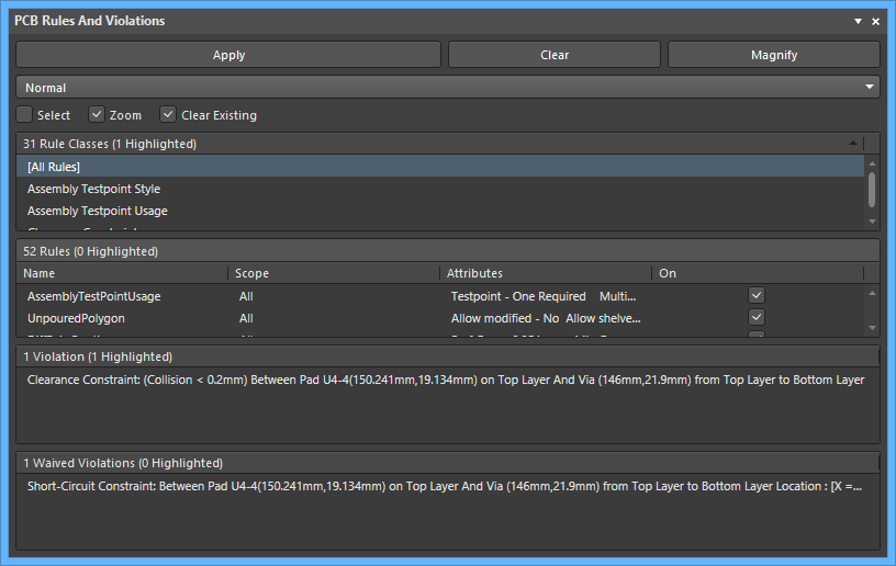
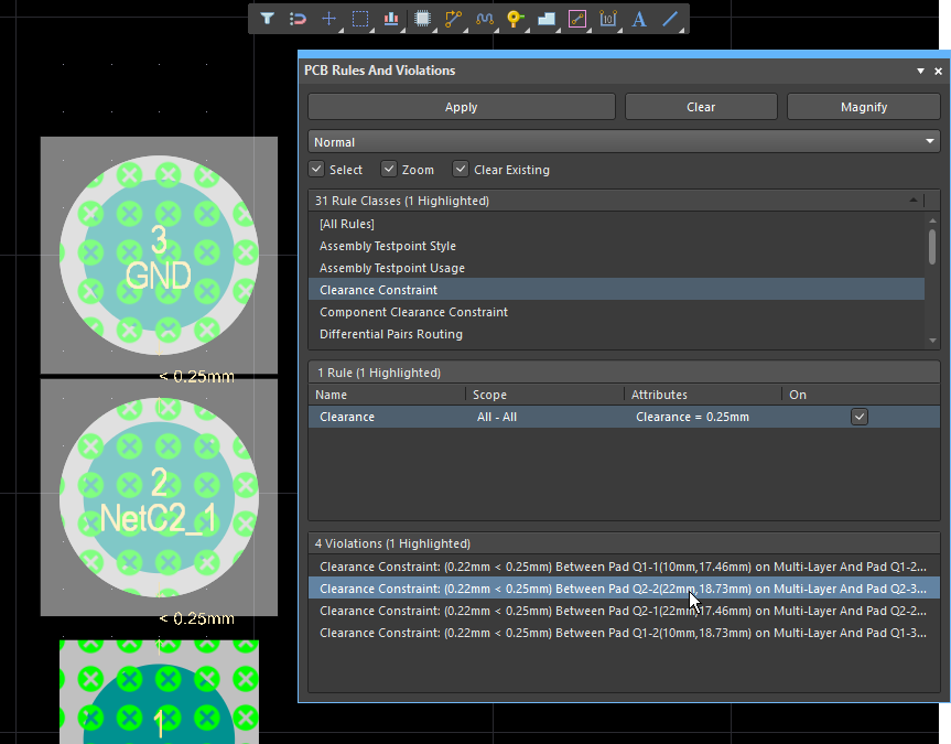
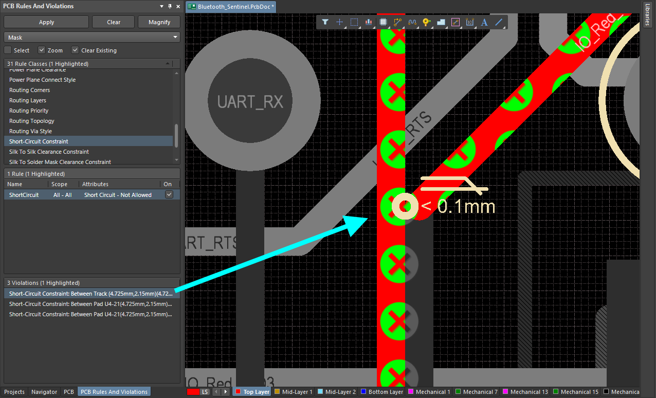
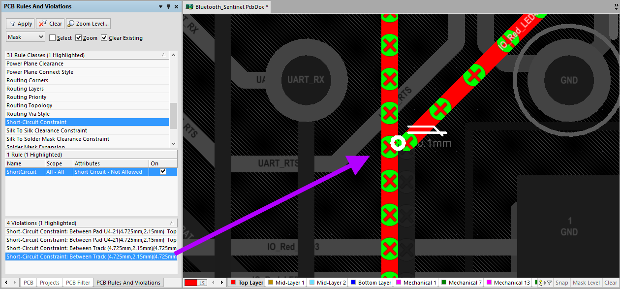
Pcb Rules And Violations Altium Designer 20 2 User Manual Documentation

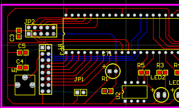
Potentially every pin on the microcomputer can be a problem.
Pcb panel design rules. These guidelines set out best practice to reduce the cost of your boards and to minimize the risk of errors arising during manufacture. Typical when a hardware designer a pcb he considers the electrical signal and the layout of the components on the circuit board focusing on the function of the product. Routed panels with different pcb composed. So if you want to separate multiple boards with v cut or milled slots please make sure each sub board is the same and less than 40 pieces sub boards per panel otherwise there may be extra processing charges.
Look at our services overview to see more details. Design guidelines to be discussed concern radio frequency rf noise from the microcomputer. In very complex boards for specialized applications. Not all possible pcb design features are available on all our services.
Pcb panel is a combination of several pcb unit boards with various possible connection modes as shown in the figures below. Mechanical processing and design parameters. The noise is present on all outputs inputs power supply and ground at all times. This noise is generated inside the device and is coupled out in many different possible ways.
Automated circuit board assembly equipment often has trouble working with smaller boards resulting in more frequent defects during the assembly process to minimize these defects and improve the throughput of the manufacturing process many companies use a process called panelization resulting in a pcb panel. Printed circuit board design rules and pcb layout guidelines become more complex as the number of layers in your stackup increases. Scoring is the preferred choice for two reasons. Not all possible pcb design features are available on all our services.
To satisfy a variety of assembly shops and pcb construction technologies the pcb design has to be more robust stronger panels more clearance of all types more robust board finishes etc. A mix panel scored and routed with different pcbs. Tn004 pcb panel design guidelines tn004 issue 6 12 july 2013 www norcott co uk 7 if a regular shaped pcb is not being panellised provision needs to be made along the longest edges of the pcb for it to be held in the smt assembly equipment. No components tracking or other mechanical feature must come within 0 200 5 00 of the edge of the pcb.
Pcb panel guidelines these guidelines set out best practice to reduce the cost of your boards and to minimize the risk of errors arising during manufacture.

Design Rules For Rigid Flex Board Hitech Circuits Co Ltd

Pcb Shapes For Panelization To Lower Cost Tempo Automation
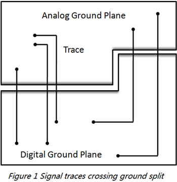
Pcb Partitioning Design Rules For Emc Improvement Pcbcart
New Pcb Design Rules Altium Designer 20 0 User Manual Documentation
Allpcb Study The Useful Rules In Pcb Layer Out Allpcb
Basic Pcb Design Rules You Should Know Latest Open Tech From Seeed Studio

Pcb Rules And Constraints Editor Online Documentation For Altium Products
From Idea To Manufacture Driving A Pcb Design Through Altium Nexus Altium Nexus 2 0 User Manual Documentation

Design Rule Checker Online Documentation For Altium Products
Design Rule Checking Altium Designer 18 1 User Manual Documentation
Design Rule Checking Altium Designer 16 0 User Manual Documentation

Altium Designer Viewer Viewing Pcb Documents Online Documentation For Altium Products
Panel Creation Multi Circuit Boards